
What Is Magnetron Sputtering and Why Is It Used in Thin-Film Deposition?
When it comes to thin-film deposition, tech like magnetron sputtering might easily be an absolutely key. The tech itself works by using gas plasma and kinetic energy to create coatings with unique properties: inside a vacuum chamber, ions bombard the target, knocking atoms free – these then deposit onto the substrate, thus forming an ultra-thin layer.
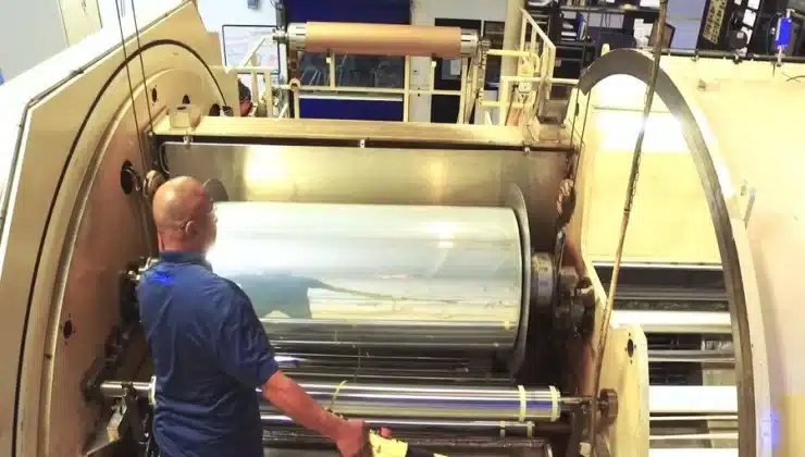
Companies like I-Photonics use the actual method to achieve top-tier results in both optics and electronics.
Magnetron Sputtering Working Principle
The process includes the following steps:
- The whole process starts with a target (the material to be sprayed) and a substrate (the surface to be coated). The chamber is first pumped to a high vacuum – to remove gases and prevent contamination. Then, a working gas (usually argon) is introduced, and the pressure is adjusted.
- A high voltage is applied between the cathode (connected to the target) and the anode (often the chamber itself), thus energizing electrons in the gas.
- Then, these very electrons collide with gas atoms, hence creating ions.
- The ions accelerate toward the target, knocking atoms loose, which then will travel through the vacuum and deposit onto the substrate, forming a thin, even coating.
- And to increase efficiency, magnets behind the target trap electrons near its surface, boosting plasma density. Lastly, reactive gases (like oxygen or nitrogen) can also be added – to adjust the chemical properties.
Advantages of Magnetron Sputtering
Unlike some other PVD methods, magnetron sputtering doesn’t need the source material to be melted or evaporated, which gives it a plenty of benefits:
- Versatility in materials. Pretty much any material can be deposited. Literally no matter how high its melting point is.
- Flexible source placement. The sources can be scaled up or down and positioned wherever needed in the chamber.
- Composition always stays true. When depositing alloys or compounds, the film’s composition stays close to that of the original source material.
Applications of Magnetron Sputtering
Magnetron sputtering is a technology that is pretty much essential in modern industries. Take solar panels, for instance: it is used to deposit thin, yet efficient layers that boost performance. The method is used to apply protective coatings on microchips, extending their lifespan.
Next, optoelectronics relies on it for anti-reflective films on screens and LED enhancement. It also enables the production of durable, transparent coatings for touchscreens and OLED displays.
Beyond electronics, the method is used in construction (e.g., tinted windows) and mechanical engineering, where wear-resistant tool coatings are essential. Without magnetron sputtering, many technologies we rely on would not be as reliable.
Magnetron sputtering is a widely used physical vapor deposition (PVD) technique for coating thin films onto surfaces. It works by creating a plasma field in which argon ions bombard a target material, causing its atoms to eject and deposit onto a substrate. The process uses a magnetic field to trap electrons, enhancing plasma density and improving efficiency. Magnetron sputtering is popular for producing high-quality coatings with excellent adhesion and uniformity, commonly used in electronics, optics, and decorative applications. It supports a variety of materials, including metals, alloys, and compounds, making it a versatile solution for advanced manufacturing and surface engineering.